
Introduction
Every smartphone, computer, and electronic device starts with a silicon wafer.
But before that wafer becomes a chip, it goes through a critical process: back grinding and thinning.
Silicon wafers start thick – typically 700-800μm. They need to be ground down to 50-100μm or even thinner for final packaging. This process must be:
-
Precise (to within a few microns)
-
Gentle (no damage to the wafer)
-
Efficient (high throughput)
-
Consistent (wafer to wafer)
The tool that makes this possible? Diamond grinding wheels – and specifically, ceramic bond diamond wheels.
In this article, we'll explain why ceramic bond diamond wheels are the go-to choice for wafer thinning, how they work, and why they're essential for modern semiconductor manufacturing.
Part 1: Why Wafer Thinning Matters
Wafer thinning, also known as back grinding, is the process of reducing a silicon wafer's thickness after device fabrication.
Why Thin Wafers?
| Benefit | Explanation |
|---|---|
| Better heat dissipation | Thinner wafers transfer heat more efficiently |
| Smaller packages | Reduced thickness allows for compact devices |
| Improved electrical performance | Shorter interconnect paths |
| Reduced stress | Thinner wafers flex more, reducing mechanical stress |
| Lower cost | More chips per wafer thickness |
The Challenge:
| Requirement | Why It's Difficult |
|---|---|
| Extreme precision | TTV (total thickness variation) <5μm |
| No damage | Subsurface damage <10μm |
| Surface finish | Roughness Ra <10nm |
| High volume | Thousands of wafers per day |
Part 2: Why Diamond for Silicon Wafer Grinding?
Silicon is hard and brittle. Only diamond abrasive is hard enough to grind it efficiently.
Abrasive Suitability:
| Abrasive | Silicon Wafer Suitability | Reason |
|---|---|---|
| Diamond | ⭐⭐⭐⭐⭐ | Hardest – efficient grinding |
| CBN | ⭐⭐⭐ | Less hard than diamond |
| Silicon Carbide | ⭐⭐ | Wears quickly |
| Alumina | ⭐ | Not suitable |
Diamond Advantages for Wafer Grinding:
| Feature | Benefit |
|---|---|
| Extreme hardness | Cuts silicon efficiently |
| Sharp cutting edges | Clean surfaces, minimal damage |
| Long life | Consistent performance over many wafers |
| Versatility | Works on various semiconductor materials |
Part 3: Why Ceramic Bond?
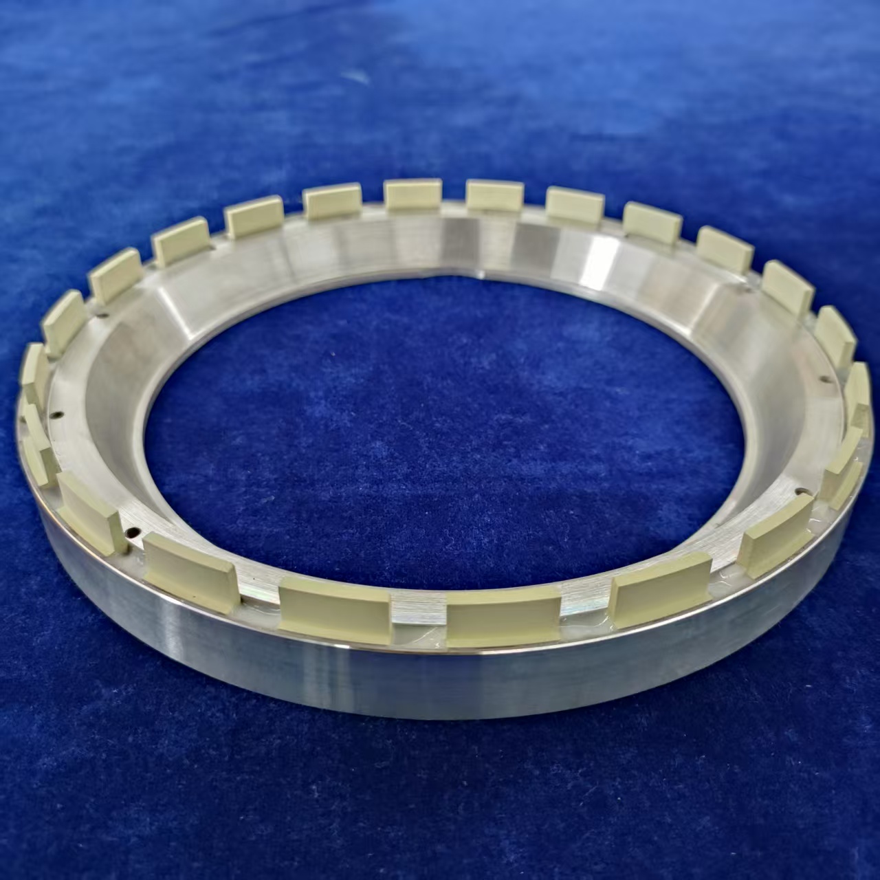
Ceramic (vitrified) bond diamond wheels offer unique advantages for silicon wafer grinding.
Bond Type Comparison:
| Bond Type | Best For | Key Characteristics |
|---|---|---|
| Ceramic / Vitrified | Coarse, semi-finish grinding | High strength, porous, self-sharpening, easy dressing |
| Resin | Fine grinding, polishing | Good finish, low grinding force, elastic |
| Metal | Heavy removal | Durable, long life, runs hotter |
Ceramic Bond Advantages for Wafer Grinding:
| Feature | Benefit |
|---|---|
| Self-sharpening | Fresh diamond continuously exposed – consistent cutting |
| Porous structure | Efficient chip removal and heat dissipation |
| Excellent form-holding | Maintains flatness – critical for TTV control |
| High wear resistance | Long wheel life – lower cost per wafer |
| Cool grinding | Low temperature – prevents wafer damage |
How Ceramic Bond Works:
| Step | Action |
|---|---|
| 1 | Diamond grains cut the silicon wafer |
| 2 |